Enabling Purity at the Nanoscale: Semiconductor Filtration Solutions
In semiconductor manufacturing, we are on the battlefield at the molecular level. Chip manufacturing processes have entered the nanoscale era, with linewidths as small as a few nanometers. At this scale, even a microscopic particle invisible to the naked eye, or an ionic impurity, can cause circuit defects on the entire wafer, resulting in enormous economic losses. Therefore, ultrapure chemicals, ultrapure water, and ultra-clean gases are no longer auxiliary conditions, but rather the lifeline determining yield and performance. Filtration and separation technologies are the core gatekeepers protecting this lifeline.
Our ultra-high purity materials precisely serve the core purification process in chip manufacturing:
Ultrapure Water Filtration System:
Application Scenarios: UPW polishing mixed beds in the final stages of chip rinsing and chemical dilution.
Specific Products: PFA/PVDF monofilament screens, serving as the support framework and filtration layer for the filter element.
Function: Effectively intercepts resin fragments and tiny particles detached from upstream, ensuring that the ultrapure water flowing into the wafer surface achieves PPT-level purity.
High-Purity Chemical Solution Filtration:
Application Scenarios: Terminal filtration of critical process liquids such as etching solutions, CMP slurries, and photolithography developers.
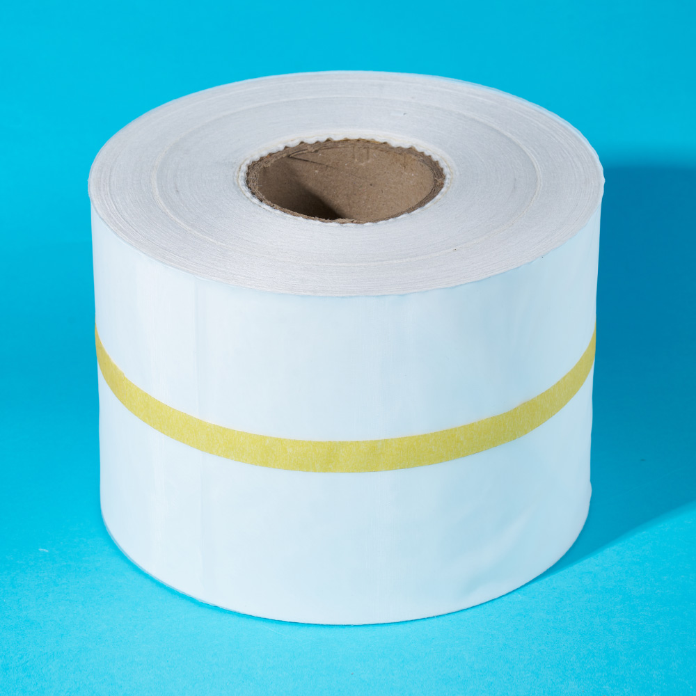
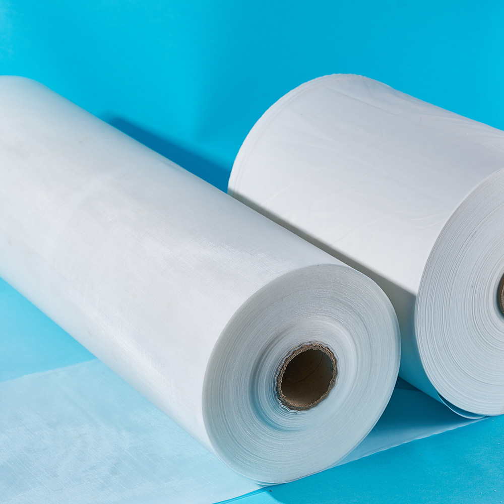
Specific Products: High-precision PFA monofilament screens and seamless woven filter cloth.
Function: Precisely filters gels, agglomerates, and metal ion contaminants in chemical solutions, preventing them from causing defects on the wafer surface and ensuring uniformity of etching and polishing.
Gas Filtration and Distribution:
Application Scenarios: Terminal purification of cleanroom environments and process gases (such as nitrogen and argon).
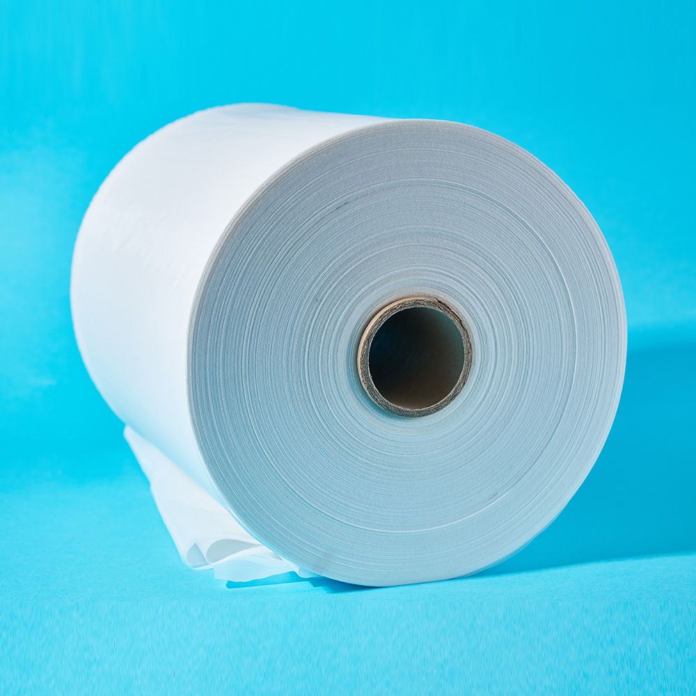
Specific Products: PTFE depth filter material.
Function: It efficiently filters out oil droplets, moisture and particulate matter from the gas, providing a "dust-free" gas source for key processes such as photolithography and thin film deposition.![]()
Choosing our semiconductor-grade filtration products means choosing an uncompromising foundation of quality:
Extremely low leaching and precipitation: Our PFA/PVDF materials undergo special purification treatment, resulting in extremely low metal ion and total organic carbon leaching rates. This ensures no secondary contamination is introduced into ultrapure fluids, guaranteeing fluid purity from the source.
Excellent chemical compatibility: Our products can withstand almost all strong acids, strong bases, strong oxidants, and organic solvents used in semiconductor manufacturing, ensuring that the filter media does not degrade, swell, or experience performance degradation under long-term contact.
Precise and consistent pore size control: Through precise weaving and rigorous quality control, we ensure a highly uniform pore size distribution in our filter materials, providing you with stable and predictable filtration accuracy and particle retention efficiency.
Compliance with the highest industry standards: Our production system and product performance strictly adhere to the relevant standards of SEMI (Semiconductor Equipment and Materials International), providing you with reliable products that can be directly integrated into the global semiconductor supply chain.

 عربى
عربى


